|
 Business Scope Business Scope
 .Professional PCB schematic design and wiring .Professional PCB schematic design and wiring
.Duplicating sample and copying boards with precision laser equipment
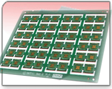
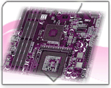
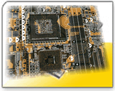
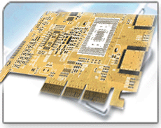
.Prefessional processing double-side and multi-layered PCB
.CAD film photographing and contraction
.Complete processing,including tin-spraying,gold plating,nickel ..plating,carbonand thickening with gold fingeroiling
.Express PCB processing service to be delivered with in 1 to 3 days while atreasonable price
.Information from the customers can be effectively sent to us through E-mail
.Delivery is possible with in the same day or the next day to the customers in the neighboring provinces,cities and Shenzhen as far as there is scheduled coach,train or flight available.
.Manufactures funded by investors of Hong Kong,Taiwan,etc.in the Pearl River Delta Region may enjoy preferential services.
.Digital drilling,trimming;computer aided testing,fully automatic copper electroplating production line.
Technical Parameters
.Board Thickness:0.4mm-3.2mms ;Maximun Processing Dimensions:1100*500mm
.Thickness of the gold plated with gold-finger:2-5U"
.Hi-Low Voltage O/S Testing:10-250V,6000 points Formation V-CUT.PUNCH.CNC
.Double-sided and multi-layered printing
.Wire width/clearance:0.13mm .Maximun taphole:0.6mm and Minimun taphole:0.25
.Minimum hole diameter:0.2mm.model precision:ˇŔ0.1mm
.Solder mask :liquid sensitizing and thermosetting
.Surface coating:nickel/gold-plated HAL
.more.
|
ˇˇ |